Potential Market Disruption by the Rising Role of Electronics Packaging
The most cost-effective way to improve computer performance for the last several decades has been to shrink the size of the transistor. Thousands of patent applications over the years have focused on exactly this approach. However, shrinking the node size is becoming increasingly less cost effective. This trend is creating more incentive for the creation of other methods to improve computer performance. For example, Taiwan Semiconducting Manufacturing Company (TSMC) has created a package on package method of packaging chips that shows performance increases comparable to an iteration of node shrinkage. Specifically, TSMC has claimed that their Integrated Fan-Out (InFO) process can realize greater than a 20% reduction in overall package thickness, a 20% speed gain, and 10% better power dissipation[1]. These benefits were recognized by Apple when InFO packaging was used in their A10 and A11 processors. TSMC increased their patent filings to 873 in 2016, which is a 74% increase over 2015, and broke into the top 10 in terms of issued US patents in 2016. Many of these filings likely relate to their disruptive new approach.
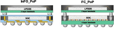
The performance benefits of InFO are created by its unique configuration. InFO is similar to a flip chip package on package arrangement. The figure below, from TSMC’s paper InFO (Wafer Level Integrated Fan-Out) Technology, shows the difference between the InFO package and a flip chip package on package. The InFO package eliminates the solder bumps which are used in the flip chip configuration to connect the chip to the laminate. Eliminating the solder bumps is a major factor in decreasing the thickness of the package.
The InFO configuration also provides more efficient signal routing. InFO makes use of different interconnection strategies that create shorter travel distances, better signal integrity, less power dissipation, and greater input/output density. The configuration also has greater thermal dissipation creating less risk of malfunction and leakage current. The interconnections and thermal dissipation will be discussed in more detail in the next post.
Furthermore, the rising importance of electronic packaging has created a change in the roles of businesses within the industry. Outsourced semiconductor assembly and test (OSAT) vendors traditionally provided chip packaging services while fabrication facilities or foundries provided the chips. However, TSMC, traditionally a foundry, has now created the InFO package and is making large investments in the second generation of the InFO package. There are further reports that other chip manufactures such as Samsung and Intel are also investing in packaging technologies. The changing market will be discussed in more detail in the third post.
The increasing difficulty of chip scaling is already creating change in the market. The increasing importance of chip packaging may be the beginning of a new trend in the computing industry.
Thanks to Sung Yi, Department Chair at Portland State University, for his knowledge on the subject.
[1] Q3 2015 Taiwan Semiconductor Manufacturing Co Ltd Earnings Call http://www.tsmc.com/uploadfile/ir/quarterly/2015/3C2bO/E/TSMC%203Q15%20transcript.pdf
The performance benefits of InFO are created by its unique configuration. InFO is similar to a flip chip package on package arrangement. The figure below, from TSMC’s paper InFO (Wafer Level Integrated Fan-Out) Technology, shows the difference between the InFO package and a flip chip package on package. The InFO package eliminates the solder bumps which are used in the flip chip configuration to connect the chip to the laminate. Eliminating the solder bumps is a major factor in decreasing the thickness of the package.

The InFO configuration also provides more efficient signal routing. InFO makes use of different interconnection strategies that create shorter travel distances, better signal integrity, less power dissipation, and greater input/output density. The configuration also has greater thermal dissipation creating less risk of malfunction and leakage current. The interconnections and thermal dissipation will be discussed in more detail in the next post.
Furthermore, the rising importance of electronic packaging has created a change in the roles of businesses within the industry. Outsourced semiconductor assembly and test (OSAT) vendors traditionally provided chip packaging services while fabrication facilities or foundries provided the chips. However, TSMC, traditionally a foundry, has now created the InFO package and is making large investments in the second generation of the InFO package. There are further reports that other chip manufactures such as Samsung and Intel are also investing in packaging technologies. The changing market will be discussed in more detail in the third post.
The increasing difficulty of chip scaling is already creating change in the market. The increasing importance of chip packaging may be the beginning of a new trend in the computing industry.
Thanks to Sung Yi, Department Chair at Portland State University, for his knowledge on the subject.
[1] Q3 2015 Taiwan Semiconductor Manufacturing Co Ltd Earnings Call http://www.tsmc.com/uploadfile/ir/quarterly/2015/3C2bO/E/TSMC%203Q15%20transcript.pdf